Testbench Automation#
Automated Generation of Clock Cycle Accurate RTL Testbenches and Test Stimulus from Timing Diagrams#
Creating Test Cases#
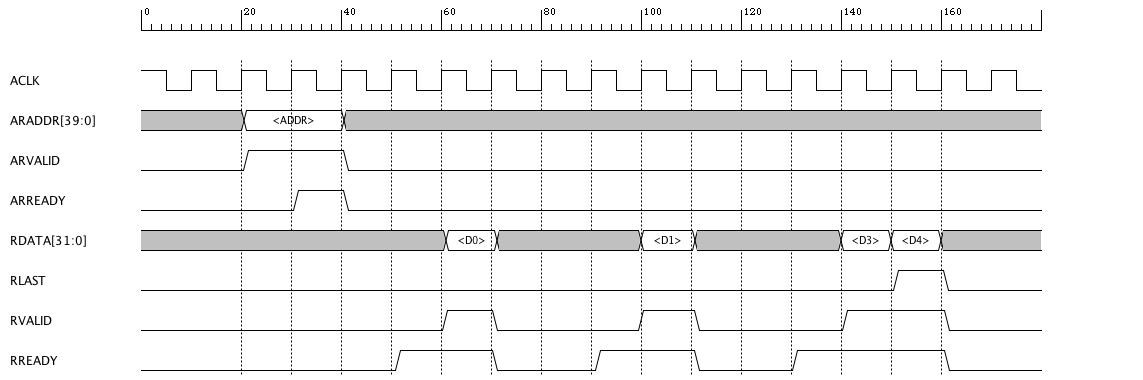
The timing diagram above shows an example of a AXI read transfer of four 32 bit words. D0, D1, D2, and D3. The read occurs at the starting address ADDR. These are variables as denoted by the < > markers.
- Testbench Outputs (AXI Master)
ACLK Clock source
ARADDR Master outputs read address
ARVALID Master outputs read address valid control signal
RREADY Master ready to read the data from the slave
- DUT Outputs (AXI Slave)
ARREADY Read address ready.
RDATA Read data.
RVALID Read data valid.
RLAST
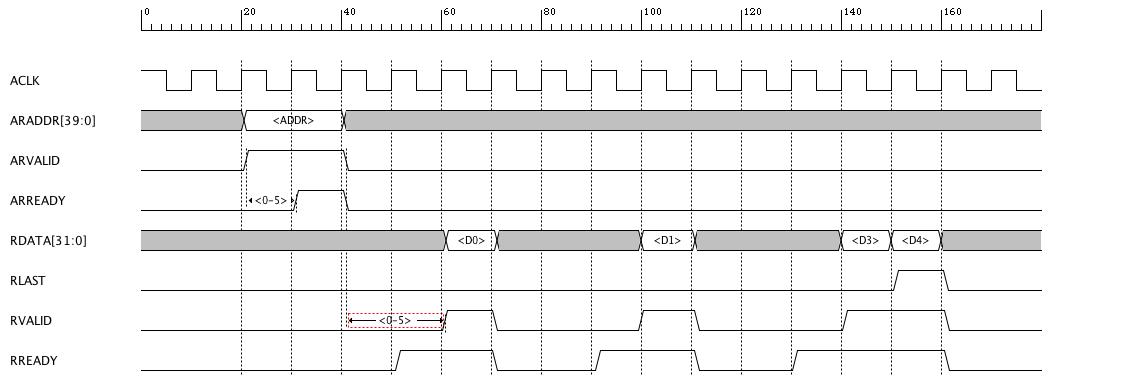
We need to annotate the diagram to specify clock cycle delays that indicate when outputs can occur (are valid) from the DUT or Testbench. I’ll show only a couple of these constraints for brevity.
VAL_2_RDY. [0-5] clock cycles from ARVALID asserted from TB
RDY_2_VLD. [0-5] clock cycles from RVALID asserted from DUT
The diagram below shows these 2 constraints. I used the Pulse Width Labels to annotate the diagram. [ ] brackets will be used for clock based constraints. Note: update app to use [ ] for the constraints.
Once the diagram is complete, you can save a test case by selecting the testbench -> “create test case” from the top menu or pop-up menu. This will cause a new panel to be displayed on the left of diagram that has input text boxes for each variable and constraint in the diagram. Test cases can be added and edited in this panel. They are saved in same .tim file as the diagram.
Test Case |
Signals |
Constraints |
|---|---|---|
axi_read_slow_mem |
ADDR = 1000 |
VAL_2_RDY = 2 |
D0 = 0000_0001 |
RDY_2_VLD = 2 |
|
D1 = 0000_0002 |
||
D2 = 0000_0003 |
||
D3 = 0000_0004 |
||
axi_read_fast_mem |
ADDR = 8000 |
VAL_2_RDY = CR |
D0 = 0001_0000 |
RDY_2_VLD = CR |
|
D1 = 0002_0000 |
||
D2 = 0003_0000 |
||
D3 = 0005_0000 |
Creating Test Suites#
A test suite is simply a list of test cases that have been created following the guide above.
Once the test cases have been created, use the top menu or pop-up menu testbench -> “create test suite”. In a panel that is displayed on the left of the diagram, test cases are added to a list that makes up the test suite. Once the test cases are added to the list, enter the name of the test suite and save it. For example: I named the test suite “mem_test” and it contains both test cases in the table above. The test suite is saved in the same timing diagram .tim file. Once the test suite is saved, a button in the panel “Generate Timing Diagram” will generate a new timing diagram in another tab that has each test case displayed in the sequence defined in the test suite with the values and constraints defined in the test cases. The new diagram filename is <test suite name>_suite.tim.
Creating Test Vectors#
Once the test suites and test cases have been created, the test vector file is created using the top menu or pop-up menu -> “Create test vectors”. This creates a test vector text file that is used by the VHDL testbench. The testbench reads DUT input signals values and compare expected DUT output values to actual DUT output values every clock cycle. Signals in the test vector file are specified in the columns while signal values are specified in each line for every clock cycle. The testbench applies the DUT input values at the specified application time and checks DUT output values at the specified observation time in the clock cycle. The example below shows the part of the test vector file created for the axi_mem test suite. The signals are shown at the top in columns followed by signal input and output definitions and then the clock cycle accurate definitions in each row for the axi_read_slow_mem test case:
                         A      A      A         R      R      R      R
                         D      R      R         D      L      V      R
                         D      V      R         A      A      A      E
                         R      A      E         T      S      L      A
                                L      A         A      T      I      D
                                I      D                       D      Y
                                D      Y
#
# DUT I/O                i      i      o         o      o      o      i
#
#
# axi_read_slow_mem test case
#
ACLK
           2             X      0      0         X       0    0    0
           1             X      0      0         X       0    0    0
           3   0_0000_1000      1      0         X       0    0    0
           4   0_0000_1000      1      1         X       0    0    0
           5             X      0      0         X       0    0    0
           6             X      0      0         X       0    0    1
           7             X      0      0 0000_0001       0    1    1
           8             X      0      0         X       0    0    0
           9             X      0      0         X       0    0    0
           10            X      0      0         X       0    0    1
           11            X      0      0 0000_0002       0    1    1
           12            X      0      0         X       0    0    0
           13            X      0      0         X       0    0    0
           14            X      0      0         X       0    0    1
           15            X      0      0 0000_0003       0    1    1
           16            X      0      0 0000_0004       1    1    1
           17            x      0      0         X       0    0    0
The VHDL Testbench#
After the test vector file has been created, the VHDL testbench is created using the top menu or pop-up menu -> “Create Testbench”. The testbench is complete and ready to use. It will parse the test vector file and create clock cycle accurate stimulus for the DUT inputs from values specified in each row and compare the actual DUT outputs to the expected DUT outputs values specified in each row.
Analog functions will be supported as well so test vectors that get created automatically will include analog signals with real values specified in each clock cycle. They can be synchronized or gated with any digital signal for start or stop times. Analog signals will be defined using common Spice time dependent sources such as PULSE, SIN, EXP, and PWL.